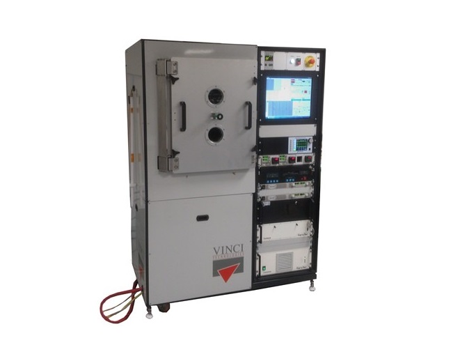
Vacuum deposition sputtering is a physical vapor deposition technique that is widely used in the semiconductor industry for depositing thin films on various substrates. It involves the use of a high-energy ion beam to sputter atoms or molecules from a target material, which are then deposited onto the substrate to form a thin film. The process takes place in a vacuum chamber, where the target material is bombarded with ions that knock off atoms or molecules from the surface. The sputtered material then travels through the vacuum chamber and deposits onto the substrate, where it forms a thin film. This technique is widely used in the production of microelectronics, flat-panel displays, and solar cells, among other applications.
PHOTIK SCIENTIFIC PVT. LTD.
Technology is the future
Phone
+91-9310249352 / +91-8605504814
+91-9310249352 / +91-8605504814
Sputtering